Click on the author name to see the abstract.
| Chair: Rafael Gutierrez | |
| 09:00-09:35 | Kurth |
| 09:35-10:00 | Kelly |
| 10:00-10:25 | Krasovskii |
| 10:25-11:00 | Coffee break |
| Chair: Andrea Donarini | |
| 11:00-11:35 | Jauho |
| 11:35-12:10 | Meunier |
| 12:10-12:35 | Garcia-Mota |
| 12:35-13:00 | Foti |
| 13:00-15:30 | Lunch break |
| Chair: Alexandre Reily Rocha | |
| 15:30-16:05 | Gutierrez |
| 16:05-16:30 | Faizy |
| 16:30-17:00 | Coffee break |
| Chair: Stefan Kurth | |
| 17:00-17:35 | Rocha |
| 17:35-18:10 | Kim |
| 18:10-18:35 | Soler |
| 21:00-23:30 | Conference dinner |
Invited talk
Steady-state density functional theory for finite bias conductances
1Dept. of Materials Physics, Univ. of the Basque Country UPV/EHU, San Sebastian, Spain
2IKERBASQUE, Basque Foundation for Science, Bilbao, Spain
3Dept. of Physics, Univ. of Rome "Tor Vergata", Rome, Italy
4INFN, Frascati, Italy
In the framework of density functional theory a formalism to describe electronic transport in the steady state is proposed which uses the density on the junction and the steady current as basic variables. In a finite window around zero bias, a one-to-one map is established between the basic variables and both local potential on as well as bias across the junction. The resulting Kohn-Sham system features two exchange-correlation (xc) potentials, a local xc potential and an xc contribution to the bias. For weakly coupled junctions the xc potentials exhibit steps in the density-current plane which are shown to be crucial to describe the Coulomb blockade diamonds. At small currents these steps emerge as the equilibrium xc discontinuity bifurcates. The formalism is applied to a model benzene junction, finding perfect agreement with the orthodox theory of Coulomb blockade.
Contributed talk
Giant room temperature interface spin Hall and inverse spin Hall effects
1 Faculty of Science and Technology and MESA+ Institute for Nanotechnology, University of Twente, P.O. Box 217, 7500 AE Enschede, The Netherlands
2 The Center for Advanced Quantum Studies and Department of Physics, Beijing Normal University,100875 Beijing, China
The spin Hall angle (SHA) is a measure of the efficiency with which a transverse spin current is generated from a charge current by the spin-orbit coupling and disorder in the spin Hall effect (SHE). In a study of the SHE for a Pt|Py (Py=Ni80Fe20) bilayer using a first-principles scattering approach, we find a SHA that increases monotonically with temperature and is proportional to the resistivity for bulk Pt. By decomposing the room temperature SHE and inverse SHE currents into bulk and interface terms, we discover a giant interface SHA that dominates the total inverse SHE current with potentially major consequences for applications [1].
To study bulk Pt, we set up a scattering geometry consisting of two crystalline semi-infinite Pt leads sandwiching a scattering region of length LPt of disordered Pt with atoms displaced from their equilibrium positions by populating phonon modes, as sketched in Fig. 1a. For the resistivity and spin-flip diffusion length, this approach has been shown to yield essentially perfect agreement with experiment [2]. We study the SHE by calculating local longitudinal and transverse charge and spin current densities in the scattering region so that both intrinsic and extrinsic contributions are naturally included. To study interface effects, we model a Py|Pt bilayer by matching 9×9 interface unit cells of Py to 3√7×3√7 unit cells of Pt [3] including both lattice and spin disorder in Py. Fig. 1b shows the results obtained for bulk Pt at room temperature. This presentation will review the computational procedures that make these calculations possible [4].
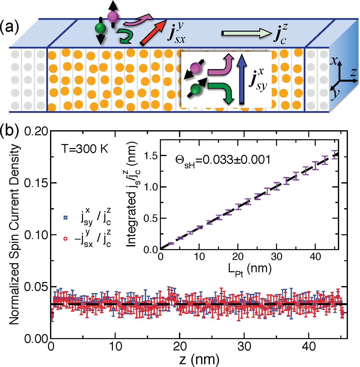
Figure 1: (a) Schematic illustration of the scattering geometry. Electrons flow jcz from the perfectly crystalline left lead to the right one through a disordered region of pure bulk Pt where atoms are displaced from their equilibrium positions by populating phonons. Transverse spin currents arising from the SHE flowing along x and -y directions are polarized in the y jsyx and jsxy directions, respectively. (b) Calculated transverse spin-current densities in Pt normalized by jcz at room temperature. The error bars are a measure of the spread of 10 random configurations of disorder. The dashed black line shows the extracted SHA. Inset: integrated spin current density in a length LPt of disordered Pt. The dashed black line illustrates a linear least squares fit from which a SHA for pure bulk Pt of ΘsH=0.033 ± 0.001 is extracted.
[1] L. Wang, R. J. H. Wesselink, Y. Liu, Z. Yuan, K. Xia and P. J. Kelly, PRL 116, (2016).
[2] Y. Liu, Z. Yuan, R. J. H. Wesselink, A. A. Starikov, M. van Schilfgaarde and PJK, PRB 91, 220405(R) (2015).
[3] Y. Liu, Z. Yuan, R. J. H. Wesselink, A. A. Starikov and P. J. Kelly, PRL 113, 207202 (2014).
[4] Z. Yuan et al., PRL 113, 266603 (2014); PRL 109, 267201 (2012); A. A. Starikov et al., PRL 105, 236601 (2010).
Contributed talk
Propagation of a Bloch-wave packet excited by a femtosecond ultraviolet pulse
1Universidad del País Vasco UPV/EHU, San Sebastián/Donostia, Spain
2Donostia International Physics Center (DIPC), San Sebastián/Donostia, Spain
3IKERBASQUE, Basque Foundation for Science, Bilbao, Spain
4Forschungszentrum Jülich and JARA, 52425 Jülich, Germany
5Christian-Albrechts-Universität zu Kiel, 24118 Kiel
6Centro de Física de Materiales, Centro Mixto CSIC-UPV/EHU, 20018 San Sebastián/Donostia, Spain
Transport properties of electron wave packets underlie the functioning of electronic devices and are an important factor in time-resolved photoemission spectroscopies. Here we consider the photoelectron motion in an attosecond streaking experiment [1] and focus on the hitherto neglected aspect: the interaction with the exciting field in the course of propagation. The non-stationary Schrödinger equation is solved numerically exactly for a model that realistically describes the lattice scattering [2]. We go beyond the standard treatment of inelastic processes with an absorbing potential and develop a microscopic approach to it.
We theoretically establish that in a crystal an optically excited electron may propagate faster than with the group velocity and faster than the free electron. The essence is that the interaction of the wave packet with the crystal lattice slows down the temporal evolution of its energy spectrum (see figure), and while the spectrum keeps changing the packet propagates faster than a packet with a stationary spectrum. At the same time, for a weak lattice scattering, the phenomenological result that the photoelectron moves with the group velocity dE/dℏk and traverses on average the distance equal to the mean free path is proved to hold even at very short travelling times. These findings offer a novel interpretation of the delay time in the streaking experiment and shed new light on tunneling in optoelectronic devices [3].
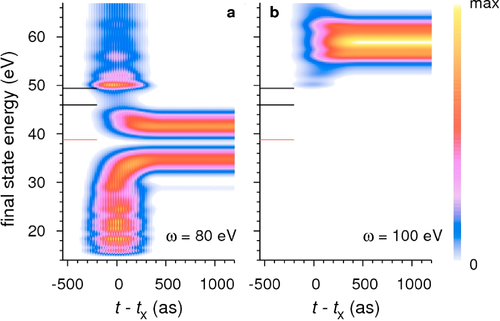
Figure: Temporal evolution of the photoelectron spectrum from a localized state at E=-41 eV excited by a light pulse of duration 1000 asec and ℏω=80 eV (a) and 100 eV (b). The gaps in the spectrum (at 39 and at 48 eV) are caused by the interaction with the crystal lattice. Owing to gaps, at 80 eV the evolution is much slower: at t=200 asec the spectrum is still spread over a range of 40 eV.
[1] A. L. Cavalieri et al., Nature 449, 1029 (2007).
[2] E. E. Krasovskii, Phys. Rev. B 84, 195106 (2011).
[3] E. E. Krasovskii, C. Friedrich, W. Schattke, and P. M. Echenique, arXiv:1506.03019 (2015).
Invited talk
Transport properties of nanostructured graphene
Center for Nanostructured Graphene (CNG), DTU Nanotech, DTU, Denmark
Despite of its many wonderful properties, pristine graphene has one major drawback: being a semimetal it does not have a band gap, which complicates its applications in electronic devices. Many routes have been suggested to overcome this difficulty, such as cutting graphene into nanoribbons, using chemical methods, or making regular nanoperforations, also known antidot lattices. All these ideas work beautifully in theory, but realizing them in the lab is very difficult because all fabrication steps induce disorder and other nonidealities, with potentially disasterous consequences for the intended device operation. In this talk I introduce these ideas and review the state-of-the-art both from the theoretical and the experimental points of view. I also introduce some new ideas, such as sublattice asymmetric doping (which Nature allows!), triangular antidots, and nanobubbles formed in graphene. Our simulations, relying on advanced numerical techniques, show that it may be possible to generate very high quality spin- and valley polarized currents with these structures – something that has not yet been achieved in the lab. Importantly, our simulations involve millions of atoms which is necessary in order to address structures feasible in the lab.
Invited talk
Modeling vertical and lateral electron transport across heterostructures
Department of Physics, Applied Physics, and Astronomy Rensselaer Polytechnic Institute, Troy, NY 12180, USA
This talk will concentrate on recent developments for the understanding of charge transport across heterostructures between nanostructured materials, including one-dimensional and two-dimensional systems.
In the first part of my talk, I will focus on electron transport taking place along heterosctructures characterized by covalent bonding [1]. I will show how controlled doping on one side of the junction can lead to device properties that are well suited for photovoltaics and photocatalysis properties.
In the second part of my talk, I will present our recent work on the role of collective motion in the ultrafast charge transfer in van der Waals heterostructures (Figure 1). [2] Using time-dependent density functional theory molecular dynamics, we find that the collective motion of excitons at the interface lead to plasma oscillations associated with optical excitation. Application to the MoS2/WS2 heterostructure yields good agreement with experiment, indicating near complete charge transfer within a timescale of 100 fs.
Finally, I will briefly present recent theoretical developments for the understanding of electronic band gap renormalization induced by substrate polarization effects, taking adsorbate size into account.
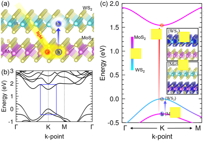
Figure 1: Atomic and electronic structures of MoS2/WS2 heterostructures. a) Illustration of the heterostructure, where a WS2 monolayer lies on top of a MoS2 monolayer. Electron and hole carriers excited by incident light separate by hole transfer onto the WS2. b) Band structure of the heterostructure, showing an indirect bandgap from Γ to K. c) Band structure in the vicinity of K-point in the Brillouin zone.
[1] J. Cai et al., Nat. Nanot. 9, 896 (2014); A. Lherbier et al., Carbon 95, 833 (2015); L. Liang and V. Meunier, J. Phys. Chem. C 119, 775 (2015).
[2] L. Liang and V. Meunier, Nanoscale 6, 5394 (2014); S. Huang et al., Nano letters 14, 5500 (2015) H. Wang et al., Nat. Comm., in press (2016).
[3] N. Kharche and V. Meunier, unpublished (2016).
Contributed talk
Integration of graphene into nanoelectronic devices: insights from atomistic simulations
1Simune Atomistic Simulations, Tolosa Hiribidea 76, 20018 Donostia-San Sebastián, Spain
2CIC Nanogune and DIPC, Tolosa Hiribidea 76, 20018 Donostia-San Sebastián, Spain; Basque Foundation for Science Ikerbasque, Bilbao, Spain; Theory of Condensed Matter, Cavendish Laboratory, University of Cambridge, J.J. Thomson Avenue, Cambridge CB3 OHE, United Kingdom
3Departament d'Enginyeria Electrònica, Universitat Autònoma de Barcelona, 08193 Bellaterra, Catalonia, Spain
4Departamento de Física de la Materia Condensada, Instituto Nicolás Cabrera (INC), and Condensed Matter Physics Center (IFIMAC), Universidad Autónoma de Madrid, Cantoblanco 28049 Madrid, Spain
The preparation of high quality graphene as host material is pivotal for further device applications. As such, a deep knowledge on the electronic and transport properties of graphene derivatives is critical to successful integration of graphene into future nanoelectronic devices. In this work, the influence of gas adsorption on the electrical characteristics of graphene, and the effect of intrinsic defects on graphene electronic properties are explored by performing Density Functional Theory (DFT) calculations using SIESTA code [1]. Contact resistance between graphene and metal electrodes is also critical for obtaining efficient graphene devices. [2] The contact resistance between graphene and various metals in different geometries is characterized by performing first-principles quantum transport calculations. The TranSiesta code [1], which implements the NEGF formalism in systems with periodic boundary conditions perpendicular to the current, is used to obtain the conductance of the suspended graphene for Pd and Al electrodes and various contact lengths.
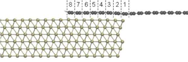
Figure 1: Structurally relaxed Pd(111)/graphene top contact, with a finite overlap (side view). Numbers indicate the amount of C atom pairs overlapping the Pd(111) contact.
[1] P. Ordejon et al. Phys. Rev. B 53, R10441 (1996); J. M. Soler, E. Artacho et al., J. Phys.: Condens. Matter 14, 2745 (2002).
[2] Fiori, G., Bonaccorso, F., Iannaccone, G., Palacios, T., Neumaier, D., Seabaugh, A., Colombo, L. Nature Nanotechnol. 9, 768 (2014).
[3] Brandbyge, M. et al. Phys. Rev. B 65, 165401 (2002).
Contributed talk
Atomic scale design of electrode terminations: gating of molecular levels in carbene-based junctions
Institute of Physics, Academy of Sciences of the Czech Republic
N-heterocyclic carbenes [1] have recently attracted much attention for their interesting optical properties and high thermal stability [2]. These characteristics make carbenes particularly attractive for possible applications in the field of molecular electronics and optoelectronics. However, a detailed study of their charge transport properties is still missing. Here we explore by means of ab-initio calculations based on density functional theory (DFT) and nonequilibrium Green's functions formalism (NEGF) the electronic and charge transport properties of a series of carbene-based molecular junctions. We focus on the effect of the geometric structure of the electrodes [3] and consider a tetramer (T), an adatom (A), a pyramid (P) and a chain-like geometry (C). We found that the LUMO level (dominating charge transport at the Fermi level) shifts by almost 0.8 eV with tip shape. This results in a strong modulation of the conductance at the Fermi level. We studied the electrostatics controlling level position for each tip geometry and rationalized these shifts in terms of the tip-dependent work function and charge rearrangement at the metal-molecule interface. We found that longer electrode terminations with a lower coordination number of the contact Au atom induce a stronger gating effect. These results open the way for the controlled modulation of the conductance in carbene-based molecular circuits.
[1] A. J. Arduengo III, R. L. Harlow, and M. Kline, J. Am. Chem. Soc. 113, 361 (1991).
[2] C. M. Crudden, J. H. Horton, I. I. Ebralidze, O. V. Zenkina, A. B. McLean, B. Drevniok, H.-B. She, Zhe Kraatz, N. J. Mosey, T. Seki, E. C. Keske, J. D. Leake, A. Rousina-Webb, and G. Wu, Nat. Chem. 6, 8 409 (2014).
[3] G. Foti and H. Vázquez, Nanotechnology 27, 125702 (2016).
Invited talk
Charge transport through dangling bond nanostructures on Si(2×1):H surfaces
1Institute for Materials Science, Dresden University of Technology, 01062 Dresden, Germany
Implementing atomic and molecular scale electronic functionalities represents one of the major challenges in current nano-electronic developments. Engineered dangling bond (DB) nanostructures on Silicon or Germanium surfaces possess the potential to provide novel routes towards the development of non-conventional electronic circuits. These structures are built by selectively removing hydrogen atoms from an otherwise fully passivated Si(100) or Ge(100) substrate. In this presentation we will address charge transport signatures of dangling bond nanostructures, covering (i) quantum interference effects in DB loops, (ii) the implementation of Boolean gates by exploiting quantum interference effects, and (iii) charge transport under the influence of a periodic time-dependent modulation, mimicking irradiation with monochromatic light. We use electronic structure methodologies to address the electronic properties of the DB nanostructures in contact with mesoscopic electrodes combined with Green's function based approaches to deal with charge transport through these nanoscale systems.
[1] A. Kleshchonok, R. Gutierrez, G. Cuniberti, Contact effects and quantum interference in engineered dangling bond loops on silicon surfaces, Nanoscale 7, 13967 (2015).
[2] A. Kleshchonok, R. Gutierrez, C. Joachim, G. Cuniberti, Quantum interference based Boolean gates in dangling bond loops on Si(100):H surfaces, Scientific Reports 5, Article number: 14136 (2015)
[3] A. Kleshchonok, R. Gutierrez, C. Joachim, G. Cuniberti, Photoassisted transport in silicon dangling bond wires, Appl. Phys. Lett. 107, 203109 (2015)
Contributed talk
Designing all simple logic gates and half-adder circuit on a Si(100)–H surface
1CEMES-CNRS, 29 rue J. Marvig, 31055 Toulouse Cedex, France
2WPI-MANA, National Institute for Material Sciences, 1-1 Namiki, Tsukuba, Ibaraki, Japan
Belonging to the Quantum Hamiltonian Computing (QHC) branch of quantum control [1-2], atomic-scale Boolean logic gates (LGs) with two inputs – one output (OR, NOR, AND, NAND, XOR, NXOR) and – two outputs (half-adder circuit) were designed on a Si(100)-(2×1)–H surface following the experimental realization of a QHC NOR gate [3] and the formal design of an half adder with 6 quantum states in the calculating block [4]. The logical inputs are determined by two nearest neighbor crossing surface Si dangling bonds, which can be, for example, activated by adding or extracting two hydrogen atoms per input. QHC circuit design rules together with semi-empirical full valence K-ESQC transport calculations were used to determine the output current intensity of the designed LGs when interconnected to the metallic nano-pads by surface atomic-scale wires. Our calculations demonstrate that the proposed devices can reach a "0" to "1" logical output ratio up to 10 000 for a running current in the 0.2 μA range for 50 mV to 150 mV bias voltage around the nano-pads Fermi level.
[1] N. Renaud and C. Joachim, Phys. Rev. A 78, 062316 (2008).
[2] W. H. Soe et al.; Phys. Rev. B 83, 155443 (2011).
[3] M. Kolmer et al.; Nanoscale 7, 12325-12330 (2015)
[4] G. Dridi, R. Julien, M. Hliwa and C. Joachim, Nanotechnology 26, 344003 (2015).
Invited talk
Simulating DNA sequencing using a combination of non-equilibrium Green's functions and QM/MM methods
Instituto de Física Teórica, Universidade Estadual Paulista (UNESP), São Paulo, SP, Brazil
The quest for rapid whole-genome sequencing using new inexpensive techniques is at the forefront of scientific research as we aim to reliably determine genetic predispositions to diseases and gain a deep understanding of our genetic code [1]. Unfortunately, currently available techniques are unlikely to reach the low cost per genome required for this procedure to become widely available in preventive healthcare [2].
Third-generation devices, in particular, sequencing with nanopores [3,4], is widely regarded as the most promising approach to enable inexpensive whole-genome sequencing and provide orders of magnitude longer base read-lengths. The fabrication of solid-state nanopores along with their envisioned application for rapid whole-genome sequencing is becoming increasingly sophisticated. However, many extremely challenging questions remain unanswered, especially how to achieve single-base resolution during polynucleotide translocation through the nanopore. One proposal is to use tunneling current across the membrane containing the nanopore and use the different electronic transport signals as a signature of the electronic structure of the different nucleotides [5].
From the theoretical point of view this is a challenging, yet exciting task. On the one hand one must simulate the dynamics of DNA as it passes through a nanopore. The molecule is surrounded by a physiological solution. At the same electrons must be explicitly tread as one wishes to calculate the current passing through the device. In this talk I will discuss recent progress in our group towards completely and realistically simulating a nanopore-based sequencing device [6]. In order to do this, I'll demonstrate how we combine quantum and classical methodologies in order to address the electronic conductance and the possibility of using graphene-based devices for single-shot DNA sequencing.
[1] F. S. Collins, E. D. Green, A. E. Guttmacher, and M. S. Guyer, Nature 422, 835 (2003).
[2] B. S. Shastry, The Pharmacogenomics Journal 6, 16 (2006).
[3] J. J. Kasianowicz, E. Brandin, D. Branton, and D. W. Deamer, Proceedings of the National Academy of Sciences of the United States of America 93, 13770 (1996).
[4] C. Dekker, Nature Nanotechnology 2, 209 (2007).
[5] M. Zwolak and M. Di Ventra, Nano Letters 5, 421 (2005).
[6] G. T. Feliciano, C. Sanz-Navarro, M. D. Coutinho-Neto, P. Ordejón, R. H. Scheicher and A. R. Rocha, Nature Communications, Phys. Rev. App. (2015).
Invited talk
Towards reality in modeling of molecule-electrode contacts
Graduate School of Energy, Environment, Water, and Sustainability (EEWS), Korea Advanced Institute of Science and Technology (KAIST), 291 Daehak-ro, Yuseong-gu, Daejeon 305-701, Korea
Molecule-electrode contacts are the critical factor that determines the characteristics of molecular electronic devices, but their atomic-scale understanding and controlling still remains elusive. In this talk, I will present several recent works within our group that are concerned with the molecule-electrode contacts. First, focusing on the ubiquitous S-Au contacts in molecular electronics, I will discuss how the single-molecule conductance is correlated with the S-Au linkage coordination number (CN). Ab initio molecular dynamics (MD) simulations show that CN three that is stable in vacuum becomes destabilized upon solvation and spontaneously converts into CN two, which will reduce the number of multiple conductance peaks robustly observed across different experimental platforms. It will be shown that our popular force fields (FFs) optimized for self-assembled monolayers [1] fail to give the correct CN-dependent conductance ordering for single-molecule junctions, and an improved FF parameterization will be presented.
In the second part, I will consider the DNA sequencing based on low-dimensional carbon nanoelectrodes. Controlling the dynamics of DNA translocation is again a central issue in the emerging solid-state DNA sequencing approach [2]. Performing large-scale FF molecular dynamics simulations, I will show that the N doping of carbon nanoelectrdoes not only increases the sensitivity and selectivity for tunneling-current nucleobase reading [3] but also benefits the control of DNA conformations by slowing down the translocation speed and reducing structural fluctuations of nucleobases.
[1] S. S. Jang et al., J. Am. Chem. Soc. 127, 1563 (2005); Y.-H. Kim et al., J. Chem. Phys. 122, 244703 (2005).
[2] H. S. Kim & Y.-H. Kim, Biosens. Bioelectron. 69, 186 (2015).
[3] H. S. Kim, S. J. Lee, & Y.-H. Kim, Small 10, 774 (2014).
Contributed talk
Modeling the conductivity of MMX molecular wires
1Dep. de Física de la Materia Condensada, Univ. Autónoma de Madrid, Spain
2Instituto de Física de la Materia Condensada (IFIMAC), Univ. Autónoma de Madrid, Spain
3Dep. de Química Inorgánica, Univ. Autónoma de Madrid, Spain
One-dimensional conductive polymers are attractive materials for flexible and transparent electronics. However, structural disorder represents a major hurdle to achieve high conductivities at both macro and nano-scales. MMX metal-organic polymers are made by a linear chain of metal and halogen atoms, bonded to lateral organic units. They have been shown to present an exceptionally high intrinsic conductivity, as well as the potential to be isolated as fibers of a few, or even a single molecular chain [1,2]. The dependence of fiber conductivity versus length depends critically on the concentration and distribution of defects, as well as on the conductance of these defects. We have studied this dependence for [Pt2I(S2CCH3)2]n wires, both experimentally and theoretically. Experimentally, we find an exponential increase of resistance with length. For nanoribbons, made by many molecular chains, such an increase can be explained by the decreasing probability of finding nondefective chains in the ribbon [3]. For individual molecular chains, however, this increase suggests a model of Anderson localization of coherent states, in a chain of weakly dispersive defects, similar to that found in nanotubes [4].
Theoretically, we have modeled nanoribbons as a lattice of low-resistivity chains, interrupted by high-resistance defects, and weakly coupled to other parallel chains. Such a model reproduces the observed dependence with ribbon length and width [3]. For few- or single-molecule chains, we study an alternative model of weak defects. Using density functional theory, we study different possible defects, extracting hopping and overlap matrices to calculate the conductance of a whole chain, with randomly placed defects.
[1] R. Mas-Balleste et al., Chem. Soc. Rev. 39, 4220 (2010).
[2] L. Welte et al., Nature Nanotech. 5, 110 (2010).
[3] C. Hermosa et al., Nature Comm. 4, 1709 (2013).
[4] C. Gómez-Navarro et al., Nature Mater. 4, 534 (2005).