Click on the author name to see the abstract.
Format: A0 portrait.
Poster
Diamondoid-based molecular devices and their electronic transport properties
Institute for Computational Physics, University of Stuttgart, Germany
In this work, we deal with the electronic transport properties across small diamond-like nanostructures, the diamondoids [1], in a gold nanogap. In our diamondoid-based devices, a small diamondoid is placed in between the two gold electrodes of the nanogap. The diamondoids are covalently bonded to the gold electrodes through two different molecules, a thiol group and a N-heterocyclic carbene [2] molecule. The transport properties of the diamondoid-based molecular device are evaluated with respect to these two binding possibilities and the size of the diamondoid. We also investigate the influence of doping the diamondoid on the properties of the molecular device. We find that using a nitrogen atom to dope the diamondoids leads to a considerable increase of the electron transmission across the device. We show the asymmetric feature of the I-V curve applying the positive and negative bias which indicates the diode like property resulting in rectification within a very small range of bias voltages. In all cases, the efficiency of the device was manifested and is discussed in view of novel nanotechnological applications. In view of these applications, our results reveal a pathway to tune the electronic transport properties of diamondoid-based molecular devices by selectively choosing their structural characteristics.
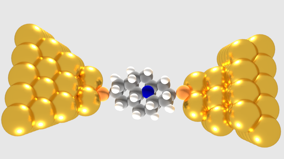
Figure 1: The setup for the transport calculations: N-doped di-thiol tetramantane embedded inside a gold nano-gap.
[1] B. Adhikari and M. Fyta, Nanotechnology 26, 035701 (2015).
[2] B. Adhikari, S. Meng, and M. Fyta, Nanoscale 8, 8966-8975 (2016).
Poster
Direct Au-C contacts based on biphenylene for single molecule circuits
Institute of Physics, Academy of Sciences of the Czech Republic
Understanding the fundamental mechanisms governing charge transport in metal-molecule-metal systems represent an essential step towards gaining control over single molecular applications. The contacts between metal and molecule strongly influence the electronic and conducting properties of molecular junctions [1]. Here we use Density-Functional Theory (DFT) and Non-Equilibrium Green's Functions (NEGF) to calculate the conductance of a biphenylene-based molecule with different chemical linkers between Au electrodes. Direct Au-C metal-molecule bonds were shown to be strong and highly-conducting [2,3]. We choose to study this molecule since it is expected that, at the gold surface, the biphenylene molecule forms stable Au-C bonds by breaking its relatively weak C-C bond. In this adsorption geometry the benzene rings are almost perpendicular to the surface. We then consider several linker groups at the other end of the molecule, which are contacted by a Au tip. In particular, we study pyridine (-C5H5N), amine (-NH2), methyl-sulfide (-SCH3) nitrile (-CN) and Au-C links and calculate the electronic and conducting properties across each of these junctions.
[1] F. Schwarz et al., J. Phys.: Condens. Matter 26, 474201 (2014).
[2] Z. L. Cheng et al., Nat. Nanotechnol 6, 353–357 (2011).
[3] W. Chen et al., J. Am. Chem. Soc. 133, 17160 (2011).
Poster
Characterization of chemically synthesized nanocomposites obtained by methylpyrrole and/or pyrrole with ZrO2 nanopowder
1Laboratoire de Chimie Organique, Macromoléculaire et des Matériaux, Université de Mascara. BP 763 Mascara 29000, Algeria
2Departamento de Química Física e Instituto Universitario de Materiales, Universidad de Alicante, Apartado 99, 03080 Alicante, Spain
The polypyrrole/ZrO2 (PP/ZrO2), poly(methylpyrrole)/ZrO2 (PMP/ZrO2) and poly(methylpyrrole-co-pyrrole)/ZrO2 (poly(MP-co-P)/ZrO2) nanocomposites has been successfully prepared via a facile chemical polymerization method. Nanopowders (ZrO2) were successfully coated with polymer through 'in-situ' chemical oxidative polymerization of pyrrole according to the procedure described elsewhere [1, 2]. X-ray diffraction analysis provides structural information. The pattern of nanocomposites (PP/ZrO2, PMP/ZrO2 and poly(MP-co-P)/ZrO2) shows the corresponding broad peak with polymer and nanopowders. UV-vis and FTIR studies showed that the ZrO2 particles affect the quinoid units along the polymer backbone and indicate strong interactions between ZrO2 and quinoidal sites of organic material. The thermal degradation behavior of polymer in the nanocomposites has been investigated by thermogravimetric analysis. The weight loss suggests that the polymer chains in the nanocomposites are more thermally stable than pristine polymer. The electrochemical behavior of the polymers extracted from the nanocomposites has been studied by cyclic voltammetry. Good electrochemical response has been observed for polymer grown into nanoparticles, the redox processes indicates that the polymer obtained in these conditions is electroactive.
Acknowledgement: This work was supported by the National Assessment and Planning Committee of the University Research (CNEPRU number E-03720130015), the Directorate General of Scientific Research and Technological Development (DGRSDT) of Algeria.
[1] I. Radja, H. Djelad, E. Morallon and A. Benyoucef, Synthetic Metals 202, 25 –32 (2015).
[2] F. Chouli, A. Zehhaf, and A. Benyoucef, Macromolecular Research 22, 26-31 (2014).
Poster
When can the Landauer formalism reproduce time-dependent transport?
University of Rochester, Rochester, NY, USA
Capturing electron transport events across molecular junctions subject to time-dependent forces or a fluctuating environment usually requires employing explicitly time-dependent techniques, such as TD-NEGF method [1], that effectively solve the time-dependent Schrödinger equation. Nevertheless, it is often desirable to approximate the time-dependent transport with steady-state techniques such as the Landauer formalism [2] by supposing that, even in the presence of time-dependent forces, the transport across the junction is in steady-state at each instant of time during the dynamics. Recently, the validity of this often-used strategy has been called into question in the context of simulations of transport through DNA in a solvent that indicate that the steady-state approximation can offer a qualitatively wrong description of the dynamics [3]. While the steady-state approach is clearly not expected to be quantitative under all modeling conditions, the practicality of the approach makes it desirable to understand the regime in which it can safely be used to model time-dependent transport phenomena.
In this work, we determine well-defined limits in which the time-dependent transport characteristics of molecules subject to a fluctuating environment can be quantitatively captured via the Landauer approach. To do so, we consider a two-level junction subject to correlated noise and contrast the time-dependent transport that results from an exact TD-NEGF method with that generated by supposing that the system is at steady-state at each instant in time. The global agreement between the two strategies is quantified by examining differences in the average currents obtained via the two methods. In turn, the ability of the steady-state approach to capture the TD-NEGF current at each instant of time is quantified by investigating the same-time correlation function of the currents obtained via the two methods. This criteria can be employed to establish an effective modeling strategy for time-dependent transport for molecules in interaction with a fluctuating environment.
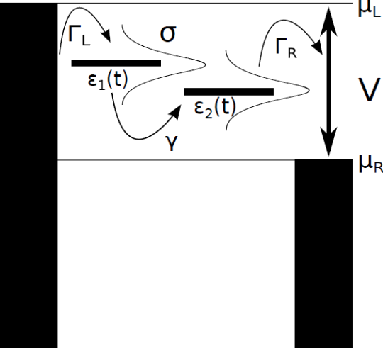
Figure 1: Two level model with correlated noise.
[1] Y. Zhang, S. Chen, and G. Chen, Phys. Rev. B 87, 085110 (2013).
[2] N. S. Meir and Y. Wingreen, PRL (1992).
[3] B. Popescu, P. B. Woiczikowski, M. Elstner, and U. Kleinekathöfer, Phys. Rev. Lett. 109, 1 (2012).
Poster
Electrons and phonons in phagraphene
1Federal University of Pará, Brazil
2Donostia International Physics Center (DIPC), Donostia-San Sebastián, Spain
3IKERBASQUE, Basque Foundation for Science, Bilbao, Spain
Recently, various carbon allotropes with sp2 and sp3 hybridization were predicted theoretically and some are candidates to show Dirac's cones [1-3]. Here we study the electron and phonon properties of one of these new allotropes of two-dimensional carbon called phagraphene, consisting of rings with 5, 6 and 7 atoms (Figure 1a) [4]. This stable structure is energetically relatively close to graphene compared to other allotropes of carbon due to its sp2 hybridization and dense atomic packing. The existence of a Dirac cone distorted in the first Brillouin zone of this structure was shown by both density functional theory (DFT) and tight-binding calculations [4].
Our investigations are based on DFT as implemented in SIESTA [5]. Electron and phonon band structures (Figure 1b,c) and density of states are computed with a finite difference scheme using Inelastica [6]. With TranSIESTA [7] we further explore electronic transport through interfaces between phagraphene and graphene (Figure 1d).
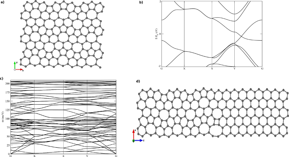
Figure 1: a) Phagraphene structure in a 3×3 repetition of the 20-atom unit cell, b) Electron band structure revealing a Dirac cone at the Fermi energy, c) Phonon band structure, d) Example of an interface structure between phagraphene and graphene for transport studies.
[1] Y. Liu, G. Wang, Q. Huang, L. Guo, and X. Chen, Phys. Rev. Lett. 108, 225505 (2012).
[2] H. Huang, Y. Li, Z. Liu, J. Wu, and W. Duan, Phys. Rev. Lett. 110, 029603 (2013).
[3] L.-C. Xu et al., Nanoscale 6, 1113 (2014).
[4] Z. Wang et al., Nano Lett. 15, 6182 (2015).
[5] J. M. Soler et al., J. Phys.: Condens. Matter 14, 2745 2002.
[7] T. Frederiksen, M. Paulsson, M. Brandbyge, and A.-P. Jauho, Phys. Rev. B 75, 205413 (2007); Inelastica software project: https://sourceforge.net/projects/inelastica.
[8] M. Brandbyge et al., Phys. Rev. B 65, 165401 (2002).
Poster
Artaios – a transport code for post-processing quantum chemical electronic structure calculations
1Institute for Inorganic and Applied Chemistry, University of Hamburg, Martin-Luther-King-Platz 6, 20146 Hamburg, Germany
2Nano-Science Center, University of Copenhagen, DK-2100 Copenhagen, Denmark
Driven by the idea of using molecules as electronic building blocks, the understanding of electron transport in molecular junctions is an important field of research. The state-of-the-art theoretical framework to investigate electron transport in the coherent regime is the Landauer–Imry–Büttiker approach [1].
We present our post-processing program Artaios [2], which is based on the Landauer approach in combination with the Green's function method [3]. Several quantum chemical electronic structure codes can be interfaced, or alternatively simple Hückel-type Hamiltonians can be post-processed. The program is capable of decomposing the transmission into local contributions (see Figure 1). The subsystem molecular orbitals can be obtained by solving the subsystems secular equations. Additionally, the program offers the possibility of calculating local spins by the Mayer local spin analysis scheme and Heisenberg exchange-spin coupling constants with a Green's function approach [4].
We incorporated several features to make user interaction as easy as possible: An easy-to-use define script can be used to setup and run transport calculations, and the program can be extended to read the output of other quantum chemistry codes.
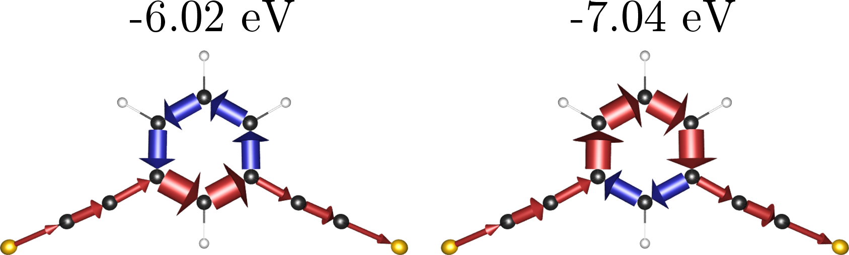
Figure 1: Local transmissions through a meta-substituted phenyl ring at energies of -6.02 eV (left) and -7.04 eV (right).
[1] M Büttiker et al., Phys. Rev. B 31, 6207 (1985).
[2] C. Herrmann et al., J. Chem. Phys. 132, 024103 (2010).
[3] Y. Xue et al., Chem. Phys. 281, 151 (2002).
[4] T. Steenbock et al., J. Chem Theory Comput. 11 (12) 5651–5664 (2015).
Poster
Molecular rectifier composed of DNA with high rectification ratio enabled by intercalation
1Single Molecule Study Laboratory, College of Engineering and Nanoscale Science and Engineering Center, University of Georgia, Athens, Georgia 30602, USA
2Department of Chemistry, Ben-Gurion University of the Negev, Beer-Sheva 84105, Israel
3Ilse-Katz Institute for Nanoscale Science and Technology, Ben-Gurion University of the Negev, Beer-Sheva 84105, Israel
The predictability, diversity and programmability of DNA make it a leading candidate for the design of functional electronic devices that use single molecules, yet its electron transport properties have not been fully elucidated. This is primarily because of a poor understanding of how the structure of DNA determines its electron transport. Here, we demonstrate a DNA-based molecular rectifier constructed by site-specific intercalation of small molecules (coralyne) into a custom-designed 11-base-pair DNA duplex. Measured current–voltage curves of the DNA-coralyne molecular junction show unexpectedly large rectification with a rectification ratio of about 15 at 1.1 V, a counter-intuitive finding considering the seemingly symmetrical molecular structure of the junction. A non-equilibrium Green's function-based model – parameterized by density functional theory calculations – revealed that the coralyne-induced spatial asymmetry in the electron state distribution caused the observed rectification. This inherent asymmetry leads to changes in the coupling of the molecular HOMO–1 level to the electrodes when an external voltage is applied, resulting in an asymmetric change in transmission.
[1] C. Guo, K. Wang, E. Zerah-Harush, J. Hamill, B. Wang, Y. Dubi & B.-Q. Xu, Nature Chemistry 8, 484–490 (2016).
Poster
Will it conduct?
1Centro de Fisica de Materiales(CFM), CSIC-UHV/EHU, San Sebastian, Spain
2Center for Nanostructured Graphene(CNG), Kgs. Lyngby, Denmark
3Donostia International Physics Center (DIPC), Donostia-San Sebastián, Spain
4IKERBASQUE, Basque Foundation for Science, Bilbao, Spain
In a recent paper [1], we have theoretically investigated the electronic properties of neutral and n- doped dangling bond (DB) quasi-one-dimensional structures (lines) in the Si(001):H and Ge(001):H substrates [2,3] with the aim of identifying atomic-scale interconnects exhibiting metallic conduction for use in on-surface circuitry. Whether neutral or doped, DB lines are prone to suffer geometrical distortions or have magnetic ground-states that render them semiconducting. However, from our study we have identified one exception – a dimer row fully stripped of hydrogen passivation. Such a DB-dimer line shows an electronic band structure which is remarkably insensitive to the doping level and, thus, it is possible to manipulate the position of the Fermi level, moving it away from the gap. Transport calculations demonstrate that the metallic conduction in the DB-dimer line can survive thermally induced disorder, but is more sensitive to imperfect patterning. In conclusion, the DB-dimer line shows remarkable stability to doping and could serve as a one-dimensional metallic conductor on n-doped samples.
Figure 1: Relaxed configuration of two different types of 1D lines on the Si/Ge(001):H substrate- color shows height of atom (black-red-orange- yellow-white). With the addition of one electron the "zigzag" pattern (A-B) undergoes distortion while the "dimer" pattern (C-D) retains its geometric and electronic structure (not shown).
Figure 2: (A-C) Relaxed structures and (D) transmission spectrum relative to the Fermi level for a DB-dimer line with different types of defects on Si(001):H.
[1] Mads Engelund et al., submitted.
[2] M. Kolmer et al., Physical Review B 86, 125307(2012).
[3] M. Kepenekian et al., Journal of Physics: Condensed Matter 25, 025503(2013).
Poster
Electron-vibration signatures in transport characteristics of graphene nanoribbons
1Center for Nanostructured Graphene (CNG), Department of Micro- and Nanotechnology, Technical University of Denmark, Ørsteds Plads, Bldg. 345E, DK-2800 Kongens Lyngby, Denmark
2Donostia International Physics Center (DIPC), Donostia-San Sebastián, Spain
3IKERBASQUE, Basque Foundation for Science, Bilbao, Spain
Electron transport was recently measured across graphene nanoribbons (GNRs) suspended between a metal surface and the tip of a scanning tunneling microscope [1]. Such lift-off experiments of GNRs from the surface open the question about propensity rules of vibrational scattering for the traversing electrons in small GNR structures.
We performed first-principles simulations of inelastic electron tunneling spectroscopy (IETS) of long pristine and defective armchair and zigzag nanoribbons under a range of charge carrier conditions [2]. For the armchair ribbons we find two robust IETS signals around 169 and 196 mV corresponding to the D and G modes of Raman spectroscopy as well as additional fingerprints due to various types of defects in the edge passivation. For the zigzag ribbons we show that the spin state strongly influences the spectrum and thus propose IETS as an indirect proof of spin polarization.
Figure 1: (a) Generic setup for an armchair GNR with a suspended part (blue shaded region) bridging semi-infinite regions in which the ribbon is thought to be in contact with a metal substrate (red shaded region) not explicitly included in the simulation. (b) Computed IETS signal for the pristine armchair GNR as a function of the dynamical region (green shaded area). Adapted from [2].
[1] M. Koch et al., Nat. Nanotechnol. 7, 713 (2012).
[2] R. B. Christensen, T. Frederiksen, and M. Brandbyge, Phys. Rev. B 91, 075434 (2015).
Poster
Probing changes in local dipole moments of non-covalently functionalized carbon nanotubes
1Institute for Inorganic and Applied Chemistry, University of Hamburg, Martin-Luther-King-Platz 6, 20146 Hamburg, Germany
2Institute for Physical Chemistry, University of Hamburg, Grindelallee 117, 20146 Hamburg, Germany
Non-covalent functionalization of carbon nanotubes (CNTs) is a useful strategy to modify and control the nanotube's electronic and transport properties, rendering them promising building blocks for designing nanoelectronic and optoelectronic devices [1].
In this work, we study the supramolecular interactions between CNTs and (among others) photoswitches using Kohn–Sham density functional theory (see Figure 1). To further clarify the involved chemical gating mechanisms, we will also present a generalized approach for the calculation of local electric dipole moments for fragments of molecular or supramolecular systems within the theory of atoms-in-molecules [2], and a new implementation in the program GenLocDip [3]. As origin-independence is achieved by relying on only few internal reference points, our approach is particularly suitable for fragments of large systems (e.g., molecules on surfaces) and may help to understand various phenomena in nanoscience, such as solvent effects on the conductance of single molecules in break junctions or the interaction between the tip and the adsorbate in atomic force microscopy.
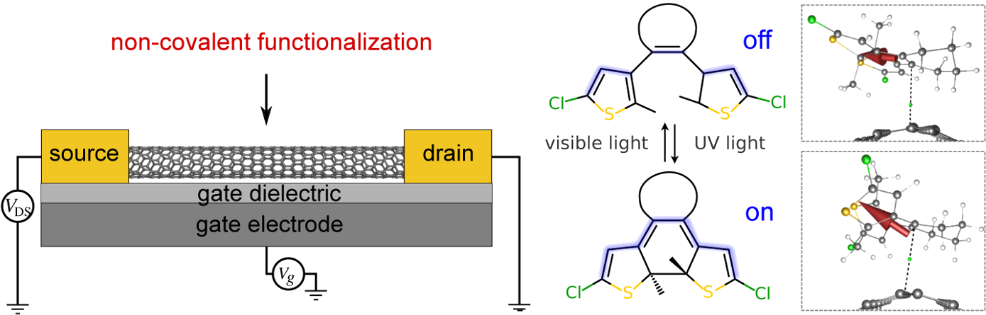
Figure 1: Left: Schematic illustration of non-covalent functionalization of a carbon nanotube field-effect transistor. Right: Photoreactivity of diarylethene photoswitches. The photoswitches' dipole moments are indicated as red arrows pointing towards the negative part (δ–).
[1] R. Waser, Nanoelectronics and Information Technology: Materials, Processes, Devices; Wiley- VCH Verlag GmbH & Co. KGaA: 2. Edition ed.; 2005.
[2] R. F. W. Bader. Atoms in Molecules: A Quantum Theory. Oxford University Press: U.K., 1990.
[3] L. Groß and C. Herrmann. GenLocDip: A program to calculate and visualize local electric dipole moments, under revision, 2016.; L. Groß and C. Herrmann. Local electric dipole moments: a flexible approach, under revision, 2016.
Poster
Scanning tunneling microscopy current from localized basis orbital density functional theory
Department of Physics, Linnaeus University, 391 82 Kalmar, Sweden
We present a method capable of calculating elastic scanning tunneling microscopy (STM) currents from localized atomic orbital density functional theory (DFT) using the Siesta code. To overcome the poor accuracy of the localized orbital description of the wave functions far away from the atoms, we propagate the wave functions, using the total DFT potential. From the propagated wave functions, the Bardeen's perturbative approach provides the tunneling current. To illustrate the method we investigate carbon monoxide adsorbed on a Cu(111) surface and recover the depression/protrusion observed experimentally with normal/CO-functionalized STM tips. The theory furthermore allows us to discuss the significance of s- and p-wave tips.
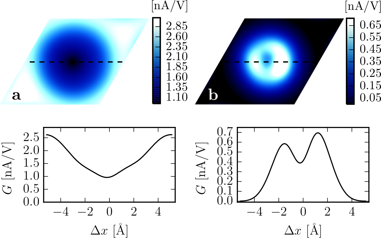
Figure 1: Comparison of the calculated constant height STM image at 5.0 Å, computed by means of a) the propagated, and b) Siesta wave functions. Bottom panel shows the cross sections along the dashed lines.
Poster
Hopping conduction and inelastic effects in molecular wires via Buttiker probes
Chemical Physics Theory Group, Department of Chemistry, University of Toronto, Canada
We explore in-detail the Landauer-Buttiker probe (LBP) technique, a simple approach that can be used to simulate electronic conduction in molecular wires. With this technique, we can phenomenologically incorporate thermal/environmental effects at trivial additional cost while replicating key physical features of conduction [1]. To demonstrate the utility of the method, we recreate experimental conditions and semi-quantitatively recover prior results to provide mechanistic information. Our simulations recover the following behavior: (i) exponential decay of conductance with molecular length, characteristic of the tunneling (superexchange) mechanism, transitioning to Ohmic-like conduction in long wires, (ii) a "Kramers-like" turnover in bath-assisted transport with respect to dephasing strength, (iii) thermal activation at high temperature, and (iv) significant fragility of on-resonance, finite bias conductance to dephasing. We also demonstrate the flexibility of the method by implementing memory (non-Markovian) effects through a structured environment.
We further extend the LBP technique into the high-bias regime and examine the role of inelastic effects on the operation of tunneling diodes [2]. We conclude that the environment has a negative impact on device efficiency, but that even with significant environmental interaction, the operation remains robust. Finally, we thoroughly explore the intrinsic differences between elastic and inelastic (dissipative) scattering methods in the near and on-resonance regimes [3], and comment on their appropriateness for simulations of molecular electronics.
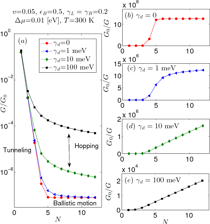
Figure 1: Tunneling-hopping turnover of the conductance with finite dephasing strength.
[1] M. Kilgour and D. Segal, J. Chem. Phys. 143, 024111 (2015).
[2] M. Kilgour and D. Segal, J. Phys. Chem. C 119, 25291 (2015).
[3] M. Kilgour and D. Segal, J. Chem. Phys. 144, 124107 (2016).
Poster
Speeding up G0W0 implementation
1Donostia International Physics Center, San Sebastian, Spain
2Centro de Fisica de Materiales, San Sebastian, Spain
Hedin's GW approximation (GWA) is a well established method of calculating the one-particle spectrum of electronic excitations. It provides a good starting point for the calculation of electron transport and optical excitation properties. A non-self-consistent version of GWA (so-called one-shot GW or G0W0) can be formulated via a one-particle Hamiltonian – the fact which simplifies the computational burden significantly. This simplification practically does not reduce the value of ab-initio predictions, especially when G0W0 calculation is started from a closely related Hartree-Fock (HF) ground state. However, even simplest G0W0 calculation remains much more cumbersome than density-functional theory (DFT) or HF calculations due to the presence of so-called screened interaction (SI). From the other hand, the G0W0 calculations of large organic molecules and molecular crystals provide a valuable information as the quality of the electronic-structure predictions is comparable with the quantum-chemistry methods based on many-electron wave functions [1].
Recently, we realized several calculations within GWA including G0W0, self-consistent GW, quasi-particle GW, all starting from the output of the DFT package SIESTA [2]. Due to an exclusive usage of real-space in representation of SI and an optimal product basis for representing SI, we were able to formulate a method with asymptotically O(N3) computational complexity, where N is number of atoms [3,4]. In this contribution, we discuss the recent advances in the method development of GWA. We are concerned now mostly with a practical walltime of execution of G0W0 calculation. This walltime can be drastically reduced i) using a contour deformation technique, ii) the availability of Lehmann representation for the non-interacting Green's function G0, iii) special product basis set optimized for the calculation of Fock-like operators. Moreover, for moderately large molecules containing several dozens of atoms, the runtime can be significantly reduced resorting to the O(N4) methods of computing the SI.
[1] Ala Aldin M. H. M. Darghouth et al. Assessment of Density-Functional Tight-Binding Ionization Potentials and Electron Affinities of Molecules of Interest for Organic Solar Cells Against First-Principles GW Calculations, Computation 3.4, 616 (2015).
[2] P. Koval, D. Foerster, and D. Sanchez-Portal, Fully self-consistent GW and quasiparticle self-consistent GW for molecules, Phys. Rev. B 89, 155417 (2014).
[3] Dietrich Foerster, Peter Koval, and Daniel Sanchez-Portal. An O(N3) implementation of Hedin's GW approximation for molecules, J. Chem. Phys. 135, 074105 (2011).
[4] Dietrich Foerster and Peter Koval, On the Kohn-Sham density response in a localized basis set, J. Chem. Phys. 131, 044103 (2009).
Poster
Electrical resistance of metal-graphene edge-contacts
1Donostia International Physics Center (DIPC), Paseo Manuel de Lardizabal 4, E-20018 San Sebastian, Spain
2Center for Nanostructured Graphene, Department of Micro- and Nanotechnology, Technical University of Denmark, Ørsteds Plads, Building 345E, DK-2800 Kongens Lyngby, Denmark
3IKERBASQUE, Basque Foundation for Science, E-48013 Bilbao, Spain
Understanding the properties of electrical contacts between bulk materials, like metals, and nanoscale structures is very important for their use in a wide variety of nanotechnology applications. Particularly, contacts of bulk metals with graphene might be of relevance in fields like electronics and spintronics. While conventional graphene-metal surface contacts have been studied extensively, graphene-metal edge-contacts are a rather new construct. Various studies demonstrate the advantages of edge-contacts over surface contacts [1,2]. However, regarding the influence of the metal on the conductance properties of edge-contacts, contrary conclusions are reached: although simulations indicate that the contact resistance for graphene-metal edge-contacts is of the same order of magnitude for different metals [2], experiments reveal a strong metal dependence [1]. To explore the origin of the differences in the reported contact resistances, we carry out transport calculations using density functional theory (DFT) ombined with a non-equilibrium Green's functions (NEGF) approach, as implemented in the TranSIESTA code. Different metals, as well as different graphene edge conformations and passivations are considered. Our results, besides clarifying the above mentioned discrepancies, will offer insights towards control of the conductance properties of graphene-metal contacts deviating from ideal interfaces.
[1] Wang et al., Science 342, 614(2013); Chu et al., ACS Nano 8, 3584(2014).
[2] Matsuda et al., J. Phys. Chem. C 114, 17845 (2010).
Poster
Currents from field-driven leads in molecular junctions: the directional photo-electric effect
Schulich Faculty of Chemistry, Technion – Israel Institute of Technology, Haifa, Israel
The study of molecular junctions and the electronic transport through them combines theoretical and experimental efforts in aim to understand these complex non-equilibrium systems and to possibly utilize them in new technological applications. A main technical difficulty that stands in our way to understand these systems regards the dynamics time scale of the electronic and nuclear motion which is still far from the time scale in which standard tools for measuring the system operate. It is therefore desired to develop a new measurement tool that would be able to probe the molecular dynamics. One approach to such new measurements is to drive molecular junctions with external electromagnetic fields.
In this work we re-derived the theory of photo assisted transport through molecular junctions on the basis of the time-independent scattering theory for time-dependent Hamiltonians. General transport formulas for field driven leads are obtained beyond some of the limitations of Tien&Gordon's formula[1]. The new formulas are tested and compared to numerical simulations for model junctions. We studied the effect of the field's parameters on the current for ac-fields and for periodic pulses and predict a "directional photo-electric effect" with promising applications, where not only the magnitude, but also the direction of photo-assisted currents can be controlled by the driving field at a given static bias voltage, see Fig.1.
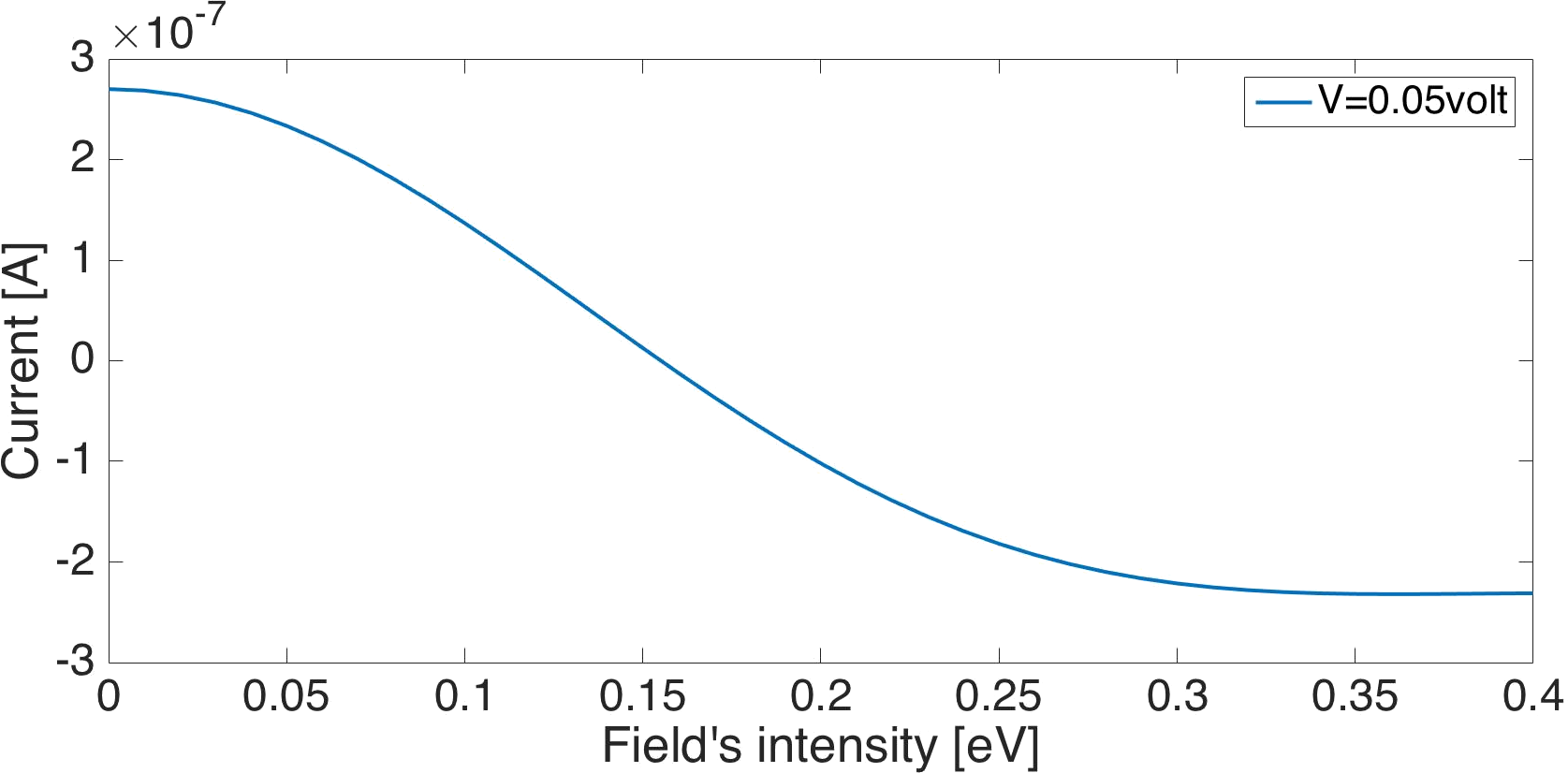
Figure 1: Photo-induced current versus field's intensity (α), for a two level molecule in a model junction, demonstrating a change of the current sign with the external field parameters.
[1] M. Kuperman, and U. Peskin, Currents from Pulse-Driven Leads in Molecular Junctions: A Time-Independent Scattering Formulation, Molecular Electronics: An Experimental and Theoretical Approach. Ed. Ioan Baldea.pp 249–280 (Pan Stanford, 2015).
Poster
Simulation of charge transport in self-assembled monolayers for applications in field-effect transistors
1Institute for Theoretical Physics and Interdisciplinary Center for Molecular Materials, University Erlangen-Nürnberg, Germany
2Computer-Chemie-Centrum and Interdisciplinary Center for Molecular Materials, University Erlangen-Nürnberg, Germany
3Organic Materials & Devices, Institute of Polymer Materials, Department of Materials Science, University Erlangen-Nürnberg, Germany
We study charge transport through self-assembled monolayers (SAMs), which are used in field-effect transistors [1,2], employing a combination of molecular-dynamics simulations, semiempirical electronic structure calculations [2] and Landauer transport theory. In particular, we investigate SAMs consisting of multifunctional molecules, where the active Π-system is linked to a flexible insulating alkyl-chain. Discussing the dependence of the transport properties on the layer composition and morphology, we find a close relation between the transport characteristics and the structural and electronic properties of the SAM [3]. For selected systems, we analyze pathways for efficient charge transport by examining local currents in the molecular layers [4]. The pathways are compared to those obtained using Metropolis Monte Carlo (MC) path searches [5]. In order to study the time-dependence of the preferred electron paths, we consider snapshots of a system selected at different times of the MD simulations. To further examine the influence of fluctuations on the transport properties, we utilize a time-dependent approach to charge transport based on time-dependent nonequilibrium Green's function (NEGF) theory [6]. This also allows for a more complete theoretical treatment, including dephasing processes.
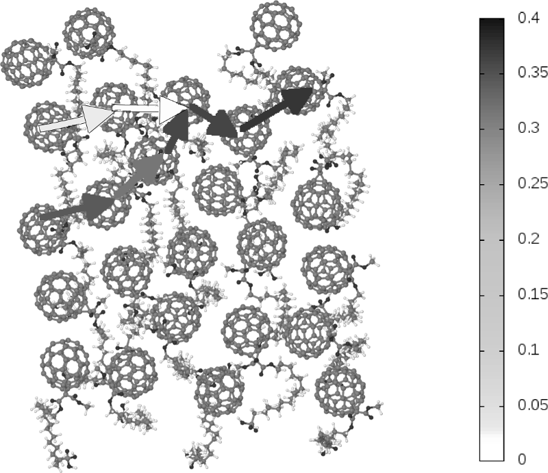
Figure 1: Transmission path through C60 SAM.
[1] M. Novak et al., Nano Lett. 114, 156 (2011).
[2] C. Jäger et al., J. Am. Chem. Soc. 135, 4893 (2013).
[3] S. Leitherer et al., J. Chem. Phys. 140, 204702 (2014).
[4] G. C. Solomon et al., Nature Chemistry 2, 223 (2010).
[5] T. Baueret al., J. Chem. Phys. 143, 044114 (2015).
[6] B. Popescu et al., Phys. Rev. Lett. 109, 176802 (2012).
Poster
Time-dependent density-functional approach for exciton binding energies
1Donostia international Physics Center, Paseo Manuel Lardizabal 4, 20018 Donostia, Spain
2Departamento de Física Aplicada II, UPV-EHU, 48940 Leioa, Spain
3Departamento de Física de la materia condensada, UPV-EHU, 48940 Leioa, Spain
Optical processes in insulators and semiconductors, including excitonic effects, can be described in principle exactly using time-dependent density-functional theory (TDDFT). Ullrich and co-workers [1,2] adapted the Casida equation formalism for molecular excitations to periodic solids, which allows to obtain exciton binding energies in a direct way. However, in this type of calculations the problem always arises from the lack of proper long-range behavior of the exchange correlation kernels in general (xc). One of the kernels proposed to overcome this issue is the well known semi-empirical Long Range Kernel (LRC) fxc(r,r')=-α/|r-r'| but its integrable singularity at r=r' as well as the slow decaying rate, need special attention particularly for periodic solids.
Recently, Sundararaman and Arias [3] developed an original method based on the Minimum Image Convention (MIC) [4] in which Coulomb type interactions are truncated on Wigner-Seitz super-cells for the calculation of exchange energies. We have implemented this numerical scheme for the direct calculation of exciton binding energies of various small- and large-gap semiconductors, as the earlier mentioned Casida formalism, resembles Fock type exchange integrals. We show preliminary results.
[1] Yang and Ullrich, Phys. Rev. B. 87, 195204 (2013).
[2] Turkowski et al., Phys. Rev. B 79, 233201 (2015).
[3] Sundararaman and Arias, Phys. Rev. B 87, 165122 (2013).
[4] Martyna and Tuckerman, The Journal of Chemical Physics 110, 2810 (1999).
Poster
Accurate classical force field for non-reactive metal-molecule interactions
1Department of Chemistry, University of Rochester, Rochester, NY 14611, USA
2Fritz-Haber-Institut der Max-Planck-Gesellschaft, Faradayweg 4-6, 14195, Berlin, Germany
Metal-molecule interactions play a determining role in molecular electronics experiments. Accurately capturing such interactions is essential in realistic simulation of state-of-the-art experiments. In particular, to obtain the statistical distribution of single-molecule events that occur in break-junction experiments, it is necessary to develop accurate and computationally inexpensive strategies that capture these essential interactions. In this paper, we introduce a transferable classical force field (FF) for non-reactive metal-molecule interactions that achieves the accuracy of high-level electronic structure methods at the cost of a classical FF computation. Specifically, the FF is composed of van der Waals (vdW) interactions, an image-charge electrostatic potential and a short-range component, and consist of just two adjustable parameters per atom type-metal pair. The simplicity of the approach is achieved by adapting recent developments [1,2] in the accurate description of vdW interactions using DFT into a classical FF. In this way, the vdW component of the FF is obtained from first-principles, and only the short-range part of the adsorption curve needs to be captured by adjustable parameters. An initial parameter set is developed via the class of planar conjugated molecules physisorbed on Au(111) shown in Figure 1. The force field is demonstrated to reproduce the adsorption profile of this class of molecules within 0.05 eV of the one obtained via DFT+vdW methods. This force field can be employed in the classical molecular dynamics simulation of the formation and evolution of molecular junctions.
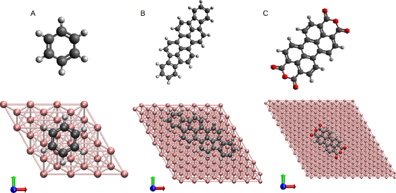
Figure 1: Three conjugated molecules adsorbed on Au(111) surfaces used for the development of the classical FF. The molecules are (A) Benzene, (B) Diindenoperylene, and (C) Perylene-3,4,9,10-tetracarboxylicdianhydrid (gold atoms are in pink, carbon in black, oxygen in red, hydrogen in light-gray).
[1] A. Tkatchenko and M. Scheffler, Phys. Rev. Lett. 102, 073005 (2009).
[2] V. G. Ruiz, W. Liu, E. Zojer, M. Scheffler, and A. Tkatchenko, Phys. Rev. Lett. 108, 146103 (2012).
Poster
Modeling of excitons in bulk rutile and the pentacene monolayer on TiO2 (110)
1Donostia International Physics Center, Paseo Manuel de Lardizabal, 4. E-20018 Donostia-San Sebastián, Spain
2Department of Physics and Materials Sciences Center, Philipps-University Marburg, Renthof 5, 35032 Marburg, Germany
3Centro de Física de Materiales CFM-MPC, Centro Mixto CSIC-UPV/EHU, Paseo Manuel de Lardizabal 5, E-20018 San Sebastián, Spain
We modeled bulk rutile and the full monolayer of pentacene adsorbed on rutile TiO2 (110) with density functional theory and computed their optical properties by solving a parametrized Hamiltonian that include the electron-hole interaction and the matter-field coupling. In bulk TiO2 we include quadrupole and magnetic dipole matrix elements that we find necessary to reproduce the experimental line shape of the Γ-point exciton. Density functional theory modeling of the pentacene monolayer on TiO2 (110) reveals a lying down, head-to-tail configuration of the molecules, with new localized states appearing in the band gap. The computed optical response shows charge transfer excitations directly from the molecular HOMO to the first TiO2 conduction bands. Exciton wave functions and binding energies are shown to be highly dependent on the dielectric screening used in the calculation.
Poster
Modeling elastic charge transfer times including the effect of structural fluctuations at hybrid organic-semiconductor interfaces
1CIC nanoGUNE, San Sebastián, Spain
2Centro de Física de Materiales, CSIC-UPV/EHU, San Sebastián, Spain
3Donostia International Physics Center, San Sebastián, Spain
4Physics Department, University of Milano-Bicocca, Milan, Italy
5Department of Chemistry, Princeton University, Princeton, New Jersey, USA
6Materials Science Department, University of Milan, Milan, Italy
Realistic descriptions of charge transfer processes at hybrid organic-semiconductor interfaces for photovoltaic applications take into account the atomic motions of adsorbates and substrates at finite temperatures. Here we present an extension of our first-principles scheme [1,2] for the extraction of elastic linewidths to model the effects of such structural fluctuations. Based on snapshots obtained from Car-Parinello molecular dynamics simulations at room temperature [3], we set up geometries in which dye molecules at interfaces are attached to a semi-infinite TiO2 substrate. We compute elastic linewidths using a Green's function method [1]. This effectively introduces the coupling to a continuum of states in the substrate. In particular we investigate the system of isonicotinic acid on rutile(110) at the level of semi-local density functional theory. We perform multiple calculations of linewidths and peak-positions associated with the adsorbate's frontier orbitals for different geometric configurations to obtain a time-averaged analysis of such physical properties. To test our theoretical model we compare our results to previously conducted core-hole clock experiments [4]. For this comparison it is necessary to include the excitonic effect in the simulation of the electronic structure. We systematically assess structural parameters affecting the interfacial charge transfer and investigate the dependence of the extracted elastic lifetimes on the relative alignment between adsorbate and substrate states.
This project has received funding from the European Union's Seventh Framework Programme under grant agreement no. 607323 [THINFACE].
[1] D. Sánchez-Portal, Prog. Surf. Sci. 82, 313 (2007).
[2] G. Fratesi et al., J. Phys. Chem. C 118, 8775 (2014).
[3] H. Lin et al., J. Phys. Chem. C 7, 3899 (2016).
[4] J. Schnadt et al., J. Chem. Phys. 119, 12462 (2003).
Poster
Application of dephasing models to molecular wires
1Bremen center for computational materials science, University of Bremen, Germany
2CNR-ISMN, Roma, Italy
We present the application of a phenomenological dephasing models based on a Non Equilibrium Green's Function formulation of electron-phonon interactions in the elastic limit. The model is applied on model hamiltonians representative of oligomers and pi-stacked wires or in combination with the Density Functional Tight Binding based DFTB+NEGF code [1,2]. We show that the processes trigerred by dephasing such as transport regime transitions, suppression of localization and diffusive transport are captured, but we will also discuss the limitations of such a simplified model. At the DFTB level, we present simulation on Quantum Interference (QI) cross-conjugated molecular wires [3]. We demonstrate a modulation of QI effects compatible with experiments and confirm the robustness of QI signatures with respect to dephasing. An analysis of the spatial localization of the dephasing process reveals that both the QI and the dephasing process are localized in the AQ region, hence justifying the general robustness of the transmission temperature dependence in different AQ based systems. The implementation in the open source library libNEGF ans possible applications are also discussed [4].
[1] A. Pecchia, G. Penazzi, L. Salvucci, A. di Carlo, New J. Phys. 10, 065022 (2008).
[2] www.dftb-plus.info.
[3] G. Penazzi et al., in submission.
Poster
Plasmonic response of metallic nanojunctions driven by single atom motion: quantum transport revealed in optics
1Centro de Física de Materiales CSIC-UPV/EHU, Paseo Manuel de Lardizabal 5, 20018 Donostia-San Sebastián, Spain
2Donostia International Physics Center (DIPC), Paseo Manuel de Lardizabal 4, 20018 Donostia-San Sebastián, Spain
The correlation between transport properties across sub-nanometric metallic gaps and the optical response of the system is a complex effect that, similarly to the near-field enhancement [1], is determined by the fine atomic-scale details of the junction structure. Using ab initio calculations, we present here a study of the simultaneous evolution of the structure and the optical response of a plasmonic junction as the particles forming the cavity, two Na380 clusters, approach and retract. Atomic reorganizations are responsible for a large hysteresis of the plasmonic response of the system, which shows a jump-to-contact instability during the approach process and the formation of an atom-sized neck across the junction during retraction. Our calculations show that, due to the quantization of the conductance in metal nanocontacts, atomic-scale reconfigurations play a crucial role in determining the optical response. We observe abrupt changes in the intensities and spectral positions of the plasmon resonances, and find a one-to-one correspondence between these jumps and those of the quantized transport as the neck cross-section diminishes. These results point out to an unforeseen connection between transport and optics at the atomic scale, which is at the frontier of current optoelectronics.
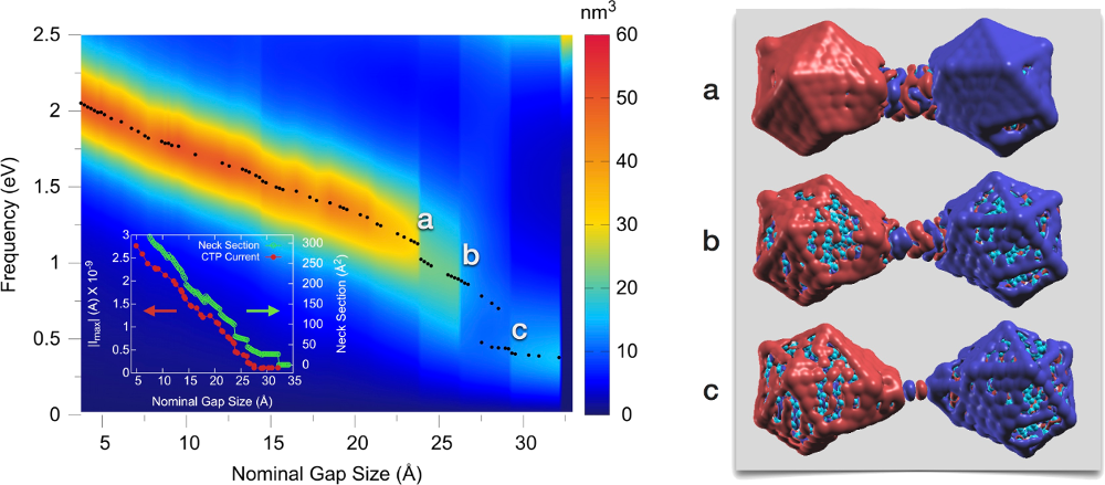
Figure 1: Left panel: Evolution of the resonances in the imaginary part of the polarizability as a function of the junction size. Due to the spontaneous formation of a metal neck across the nanojunction, we can observe a characteristic charge transfer plasmon (CTP) mode all the way up to ~30 Å nominal separations. The inset shows the electric current flowing through the junction (at the frequency of the CTP resonance), and the evolution of the cross-section of the neck. There is a one-to-one correspondence between the jumps observed in the current, in the neck cross-section and in the far-field optical response of the plasmonic cavity. Right panels: Structure of the system at the separations indicated as (a), (b) and (c) in the left panel. Imaginary part of the induced electronic charge distribution at the CTP resonance frequency for each of the configurations is also plotted (different colors indicate charge accumulation and charge depletion).
[1] M. Barbry et al., Nano Letters 354, 216 (2015).
[2] F. Marchesin et al., ACS Photonics 3, 269 (2016).
Poster
Multi-scale modeling of spin transport in organic semiconductors
1Johannes Gubenberg University, Mainz, Germany
2Texas A&M University, College Station, Texas USA
3Max Planck Institute, Mainz, Germany
Since the discovery of magnetoresistance in organic spin-valves [1], organic spintronics has been an active area of research. Organic semiconductors (OSC) show great potential for applications in next generation electronic devices due to their weak spin-orbit coupling and hyperfine interactions which leads to much longer spin life times when compared to their inorganic counterparts.
In this work, we present our development based on the VOTCA [2] toolkit for charge transport of a multi-scale modeling framework for spin transport in bulk organic materials.
By combining several techniques e.g. molecular dynamics, density functional theory and kinetic Monte Carlo, we are able to study spin transport by including thermal effects, magnetic and electric field effects in realistic morphologies of amorphous organic systems. We apply our multi-scale approach to investigate the spin transport in amorphous Alq3 [Tris(8-hydroxyquinolinato)aluminum] and address the underlying spin relaxation mechanism in this system as a function of temperature.
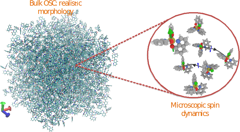
Figure 1: Realistic morphology of an amorphous Alq3 sample used to calculate the charge and spin dynamics.
[1] Z. H. Xiong et al., Nature (London) 427, 821, (2004).
[2] V. Ruehle et al., J. Chem. Theory Compt. 7, 3345 (2011).
Poster
Electronic transport in B-N substituted bilayer graphene nano-junction
1CNR, National Research Council of Italy, ISTM, via Golgi 19, Milan, Italy
2Physics Department, University of Milan-Bicocca, P.zza della Scienza 3, Milan, Italy
3Physics Department, University of Milan, via Celoria 16, Milan, Italy
We investigated a suspended bilayer graphene [1] where the bottom/top layer is doped by boron/nitrogen substitutional atoms. By using density functional theory calculations, we found that at high dopant concentration (one B-N pair every 32 C atoms) the electronic structure of the bilayer does not depend on the B-N distance but on the relative occupation of the bilayer graphene sub-lattices by B and N. The presence of the dopants and the consequent charge transfer establish a built-in electric field between the layers, giving rise to an energy gap [2].
We further investigated the electronic transport properties using the TranSIESTA code [3], which combines the non-equilibrium Green's function (NEGF) technique with DFT. We found that intra-layer current is weakly influenced by the presence of these dopants while the inter-layer one is enhanced for biases allowing an easy tunneling between layers. In order to study the role played by the dopants on the inter-layer current, we also consider a “shingle” nano-junction where the contact is made by overimposing the terminations of two semi-infinite H-terminated graphene layers. The contact region is hence constituted by partial overlap of doped graphene flakes. In this case the electron current can only flow from one graphene layer to the other, overcoming an energy barrier represented by the vacuum region in between the two flakes. This system breaks the left-right symmetry and can behave like a p-n nano-junction.
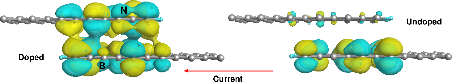
Figure 1: Eigenchannels at the Fermi level for the doped "shingle" nano-junction (left panel) and for the corresponding undoped case (right panel). The applied bias is –1.5 V.
[1] Y. Zhang et al., Nature 459, 820 (2009).
[2] J. Nilsson et al., Phys. Rev. Lett. 97, 266801 (2006).
[3] M. Brandbyge et al., Phys. Rev. B 65, 165401 (2002).
Poster
Temperature effects on orthorhombic GeS
1Istituto di Struttura della Materia of the National Research Council, Via Salaria Km 29.3, I-00016 Monterotondo Stazione, Italy
2European Theoretical Spectroscopy Facilities (ETSF)
3Instituto de Física Teórica, Universidade Estadual Paulista (UNESP), Rua Dr. Bento T. Ferraz, 271, São Paulo, SP 01140-070, Brazil
Group IV chalcogenides such as GeS, SnS, SnSe and GeSe, possess layered crystalline structures that resemble the one of black phosphorus (BP). In contrast to BP, they possess band gaps that cover the energy window from 0.9 to 1.7 eV which make them attractive for a number applications. For instance, recently SnSe has been proposed as an promissory material for thermoelectric applications as high figure of merit (ZT >2) have been found, at specific conditions of temperature and crystal orientation [1]. In addition, GeS and SnS the largest band gap among the chalcogenides, possess promising features as absorber materials and could be integrated in the design of high efficient photovoltaic cells [2]. Thus, the correct understanding of temperature on the electronic and optical properties of these chalcogenides is necessary to provide further insights regarding their applicability in photovoltaics.
In this work, we study the temperature effects on the electronic and optical properties of orthorhombic GeS. The temperature effects on the electronic states are treated in an ab-initio way within the Many-Body Perturbation Theory (MBPT) framework. There, the electron-phonon coupling which is composed by the first and second order Taylor expansion in the nuclear displacement, is treated perturbatively. Our results indicates a zero-point energy motion of ~ 36 meV. In addition, by combining the electron-phonon linewidth with the excitonic effects, we are able to study the optical absorption at finite temperatures. Our results for optical absorption are compared with ellipsometric measurements showing excellent agreement.
[1] L.-D. hao, et al. Nature 508, 373377 (2014).
[2] K. R. Reddy, N. K. Reddy, and R. Miles, Sol. Energy Mater. Sol. C. 90, 3041 (2006).
Poster
Switching the conductance of graphene-molecule junctions by proton transfer
Institute of Theoretical Physics, University of Erlangen-Nuremberg, Germany
The possibility of using single molecule junctions as components of nanoelectronic devices has motivated intensive experimental and theoretical research on the conductance properties of these systems. Recently, it has been suggested that it is possible to switch the conductance of a molecular junction by means of a proton transfer reaction triggered by an external electrostatic field [1,2]. Specifically, it has been shown that a molecular bridge, which exhibits two tautomeric forms with different conductance, can realize the "on" and "off" states of the switch. An external electrostatic field can be used to control the state of the junction in a reversible way. In this contribution, we analyze the detailed mechanism of the switching process in a molecular junction that uses graphene as material for the electrodes. Using density functional theory, we characterize the reaction path of the concerted and step-wise proton transfer processes and analyze how these different mechanisms affect the switching process. Our transport simulations performed using density functional theory and the non-equilibrium Green's function method [3] show the different conductance properties of the two states of the switch (see Fig. 1) and explain how they emerge from the electronic structure of the molecule.
Figure 1: Current-voltage characteristics for the different junctions investigated (the two insets at the top show the low and high conducting forms of the molecular bridge).
[1] C. Hofmeister et al., J. Mol. Model. 20, 2163 (2014).
[2] D. Weckbecker et al., manuscript in preparation.
[3] M. Brandbyge et al., Phys. Rev. B 65, 165401 (2002).
Poster
Quasi-one-dimensional states in rippled graphene
Faculty of Physical Sciences, National University of San Marcos, P.O. Box 14-0149, Lima 14, Peru
Graphene is a two-dimensional crystal with honeycomb-like structure from carbon atoms. Their electronic properties are strongly related to structural perfection. So, It has a high electrical mobility (10,000 cm2 / V.s at T = 300K) [1] and has a band structure described by linear dispersion relation at low energy, similar to mass-less Dirac-Weyl fermions [2]. We calculate the ballistic electron transport through nano-ripple of graphene. The curvature of the surface correspond to two directions crystallographic zigzag and armchair. We find the formation of electron transport channels that allow the quantization of the conductance, similar to that presented in graphene nano-ribbons. The results suggest a mechanism for controlling the electrical conductance by the formation of periodic nano-ripple arrays.
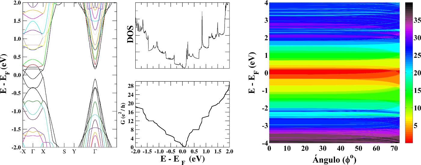
Figure 1: (Left) Band structure, DOS and conductance (G) for a periodic nano-ripple with "edge" armchair. The calculation of G display a well-defined quantization for energy around E-EF = -1.4 eV, 0.5 eV and 1.5 eV. For these energies the conductance map (right) indicate constant values independent of the angle Φ (angle Φ = tan-1(ky/kx)).
[1] Y. Zhang et al., Acc. Chem. Res. 46 (10), 2329–2339 (2013).
[2] M. Pudlak, et al., Phys. Rev. B 92, 205432 (2015).
Two poster prizes of 100 EUR each, sponsored by QuantumWise, were awarded to Susanne Leitherer and Amaury de Melo Souza.