Invited talk
Quantum transport properties across different chemical decorations in layered materials
Argonne National Laboratory, Lemont, Illinois 60439, USA
New materials with greater capabilities are a key component in the strategy to further the performance of current electronic devices. Of the limited available base options, light element layered materials are among the most promising solutions for high-performance charge transport with low heat dissipation. But the small or the absence of an electronic band gap in materials such as graphene prevents the creation of an on-to-off switch, hindering their integration in today's electronics. Within this setting, and motivated by prospects of integrating layered compounds into electronic devices to reduce consumer power consumption, I will describe how various types of chemical modifications and structural disorder in bilayer graphene [1], double-walled nanotubes [2] , as well as some new 2D materials such as black phosphorus [3] and silicene [4] can enlarge the small or non-existing electronic band gaps while preserving a good charge mobility. I will discuss the required chemistry criteria for each material, which are obtained using a combination of electronic-structure and quantum transport computational methods at the micro-meter scale, to select the type of external defect and stoichiometry for achieving specific transport profiles.
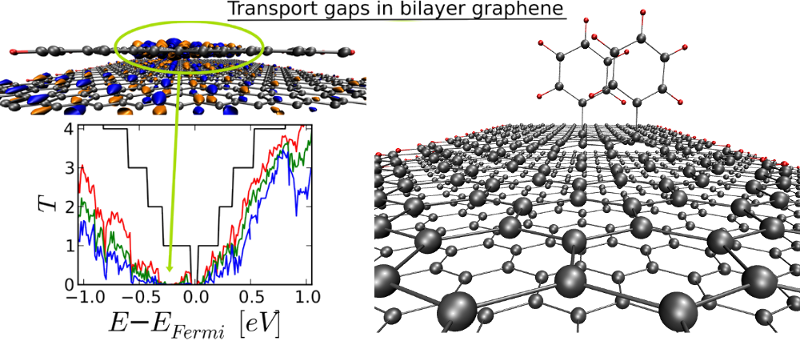
Figure 1: Defected bilayer graphene yields homogeneous transport profiles across different chemical modifications.
[1] A.Lopez-Bezanilla, J. Phys. Chem. C 118, 29467 (2014).
[2] A.Lopez-Bezanilla, J. Phys. Chem. C 118, 1472 (2014).
[3] A.Lopez-Bezanilla, Phys. Rev. B 93, 035433 (2016).
[4] A.Lopez-Bezanilla, Phys. Chem. C 118, 18788 (2014).